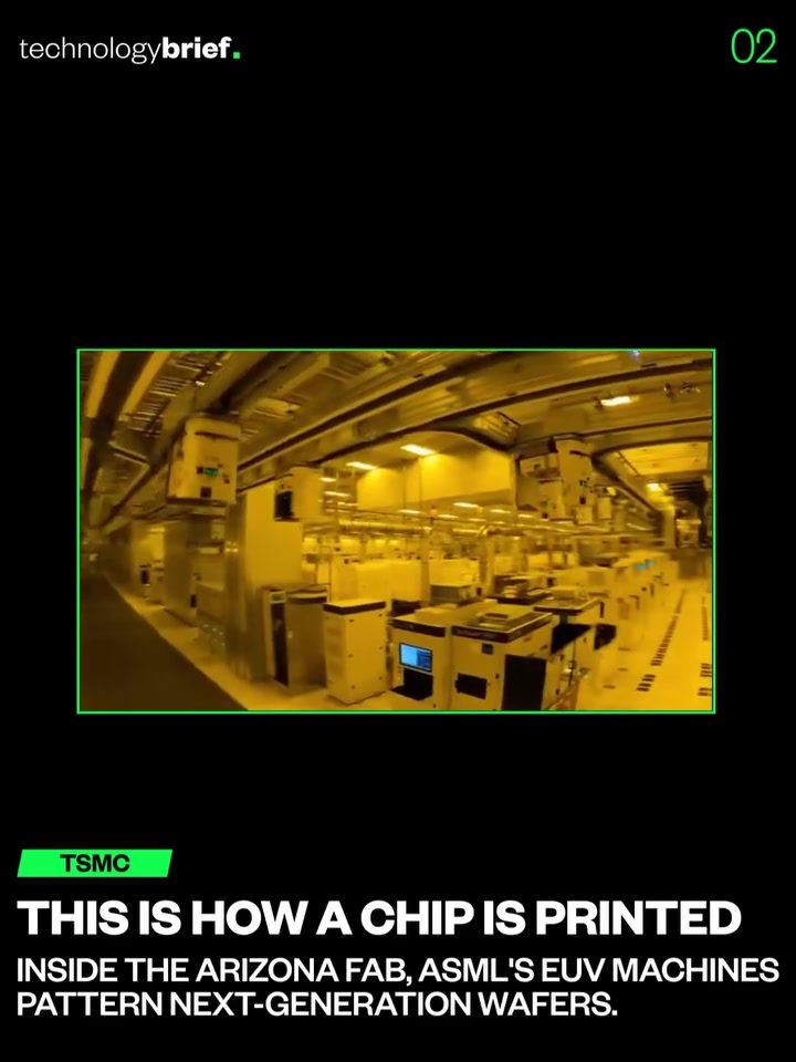
TSMC's Arizona Chip Fab: A Closer Look at Advanced Chip Manufacturing
The TSMC Arizona chip fab is a marvel of modern engineering, showcasing the intricate and cutting-edge processes involved in manufacturing advanced semiconductor chips. This facility is part of a $165 billion project aimed at bringing advanced chip manufacturing back to the United States, with plans for three fabs, a packaging plant, and an R&D center by the end of the decade. The scale of the operation is immense, with around 3,000 people already employed there.
Why This Matters
The production of semiconductor chips is a complex and highly technical process, essential for the development of modern electronics. Understanding the manufacturing process provides insights into the technological advancements and the sheer magnitude of the effort required to produce the tiny, powerful chips that power today's devices.
Inside the Fab: Automated Material Handling and EUV Machines
The Automated Material Handling System
The TSMC Arizona fab features an automated material handling system that is both efficient and impressive. The first hallway, called the "silver highway," is a critical component of this system. Approximately 700 unified pods move around the fab, carrying wafers through the factory floor on overhead rails. These pods are essential for transporting wafers to various processing stations without human intervention, ensuring a clean and controlled environment.
This automated system not only speeds up the production process but also minimizes the risk of contamination. The pods zip around, going to different tools and dropping off wafers, ensuring that the entire process is highly efficient and precise.
EUV Machines: The Heart of Chip Manufacturing
One of the most fascinating aspects of the TSMC Arizona fab is the use of EUV (Extreme Ultraviolet) machines. These machines play a crucial role in the chip manufacturing process. EUV machines create the light needed to print tiny patterns onto silicon wafers by firing lasers at droplets of molten tin tens of thousands of times per second. This process, while sounding extraordinary, is integral to producing some of the world’s most advanced chips.
The EUV machines used at the Arizona fab are provided by ASML. These machines are at the forefront of lithography technology, allowing for the creation of intricate patterns on silicon wafers. The precision and speed of these machines are critical for producing next-generation chips, which require extremely small and detailed circuitry.
The process of creating a semiconductor is a fascinating blend of high technology and precision engineering. Inside each machine, plasma ignites, and molecules and atoms move around, shaping the silicon wafers into functional chips. The result is the ability to fit billions of transistors on a single chip, enabling the development of powerful and efficient electronic devices.
The Importance of Clean Rooms
The TSMC Arizona fab is characterized by its massive clean rooms, which are essential for the chip manufacturing process. These clean rooms maintain a controlled environment to prevent contamination, ensuring the purity of the wafers as they move through various stages of production. The cleanliness of these rooms is crucial for the integrity of the chips, as even the smallest particles can impact the final product.
Practical Tips for Understanding Chip Manufacturing
For those interested in understanding the chip manufacturing process, it's helpful to focus on a few key points:
- Automation: The use of automated systems, such as the unified pods, is critical for maintaining efficiency and cleanliness in the production process.
- Advanced Technology: Technologies like EUV lithography are essential for producing next-generation chips. Understanding how these technologies work can provide deeper insights into the manufacturing process.
- Cleanliness: The clean rooms and controlled environments are vital for ensuring the quality and purity of the chips.
For anyone involved in the semiconductor industry, visiting a fab like the TSMC Arizona facility can be an eye-opening experience. It highlights the importance of precision, automation, and advanced technology in the production of modern electronic devices.
Important Takeaways
- Scale and Efficiency: The TSMC Arizona fab operates on a massive scale, with automated systems and clean rooms ensuring efficiency and quality.
- Technological Advancements: The use of EUV machines and other advanced technologies is crucial for producing next-generation chips.
- Precision and Control: The controlled environment and precise handling of wafers are essential for the integrity of the final product.
Conclusion
The TSMC Arizona chip fab is a testament to the advancements in semiconductor manufacturing. From the automated material handling system to the use of EUV machines, every aspect of the process is designed for precision and efficiency. As the industry continues to evolve, understanding these processes will be increasingly important for anyone involved in or interested in the world of technology.
Watch the Reel
Questions readers ask
What is the TSMC Arizona fab and why is it significant?
The TSMC Arizona fab is a state-of-the-art semiconductor manufacturing facility in Arizona. It's significant because it represents TSMC's effort to establish advanced chip making in the United States, reducing reliance on overseas production and enhancing domestic supply chains.
What are the key features of the TSMC Arizona chip manufacturing process?
The TSMC Arizona chip manufacturing process utilizes cutting-edge technology, including EUV (Extreme Ultraviolet) lithography, to produce high-performance semiconductor chips. The process is characterized by high precision and advanced automation to ensure consistency and efficiency.
How many facilities are planned as part of TSMC's Arizona project?
TSMC's Arizona project includes plans for three major facilities, including a packaging plant and an R&D center, alongside the initial fabrication plant. This comprehensive approach aims to create a robust semiconductor ecosystem in the United States.
What kind of automation is used in the TSMC Arizona fab?
The TSMC Arizona fab employs sophisticated automation systems throughout its chip production line, ensuring precise control over every step of the manufacturing process. This automation helps maintain high standards of quality and efficiency in the production of semiconductor chips.
What role does EUV lithography play in TSMC's chip making process?
EUV lithography is a crucial technology used in TSMC's chip making process at the Arizona facility. It allows for the creation of incredibly small and precise circuit patterns on wafers, enabling the production of advanced, high-performance semiconductor chips.
How does the TSMC Arizona fab contribute to the local economy?
The TSMC Arizona fab is a major economic driver for the region, employing around 3,000 people. As the facility ramps up to full production, it will create even more job opportunities, fostering local economic growth and development.
Related deep dives
Similar reads based on topic and creator.




Recent articles
Fresh deep dives from the latest Reels we unpacked.




Comments
Be the first to comment.