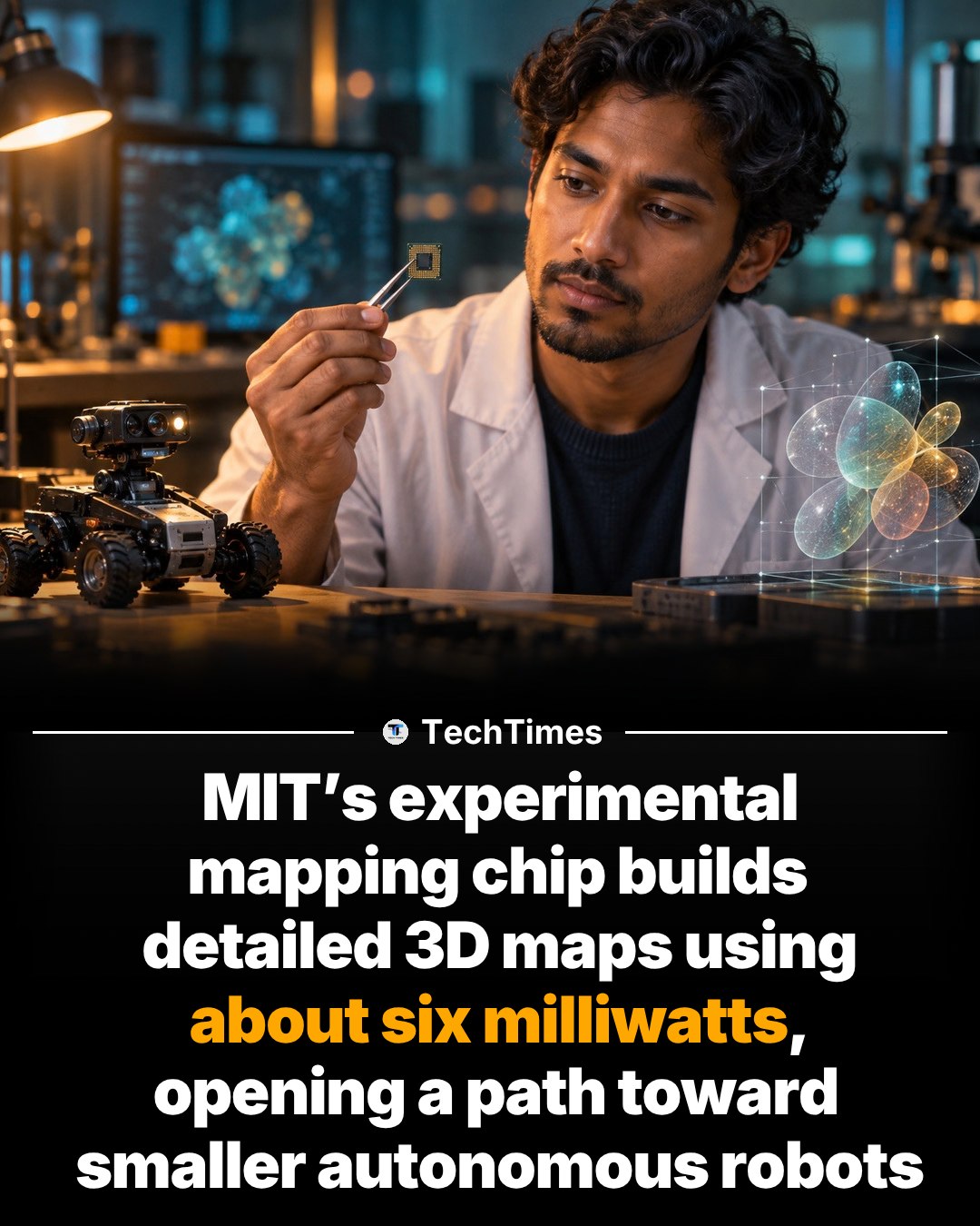
MIT researchers have developed a experimental chip that consumes roughly six milliwatts of power and builds detailed 3D maps, cutting energy consumption so low that it could dramatically shrink autonomous robotics. The MIT chip is far smaller and far more efficient than any other 3D mapping hardware, and in part because of the power savings, MIT says the chip could open a path toward smaller autonomous robots.
The MIT Mapping Chip
The experimental chip creates detailed 3D maps. “It opens a path toward smaller autonomous robots.” MIT’s chip does more than just build 3D maps; it does so with unprecedented efficiency, using only around 6 milliwatts of power. That energy consumption is a fraction of what other 3D mapping hardware requires, making this new chip a significant breakthrough in the field of autonomous robots. This is only a simple example of what MIT's mapping chip can do for autonomous robots, but it's the beginning of something exciting. This is possible using what's known as Phase change memory and complementary metal-oxide-semiconductor features. Complementary metal-oxide-semiconductor, also called CMOS is a type of integrated circuit chip used in computer processors and semiconductor devices. This is a technology that has been used for a long time in electronics. CMOS-based circuit is widely used in energy saving and high-performance applications. Phase change memory is a type of non-volatile random-access memory. Phase change memory is a non-volatile random-access memory. It is a type of memory that does not require a power source to retain information. It uses a material that can switch between two different phases, each with distinct electrical properties. This allows it to store data even when the power is turned off. Phase change memory technology is used in a variety of applications, including data storage, computer memory, and embedded systems. The technology is known for its high speed, low power consumption, and high endurance.
Imagining Smaller Autonomous Robots
The implications for the future of autonomous robotics are clear. If robots require less power to navigate and map their environments, they can be made smaller and more efficient. This could lead to a new wave of miniature robots capable of tasks previously impossible due to power constraints. Picture swarms of tiny robots exploring disaster zones, mapping out structures, or even performing microsurgery. Smaller robots would also be less obtrusive and more accessible, opening up new possibilities for domestic and industrial use. The biggest advantage of smaller autonomous robots are that they would take up less space. They would also be easier to transport and store, and they would require less energy to operate. This could make them more affordable and more convenient to use. Smaller autonomous robots would also be less likely to damage their surroundings, and they would be less likely to be noticed by people.
Why smaller robots?
Development
The MIT chip stands out for an experimental integration with phase change memory and complementary metal-oxide-semiconductor technology. These technologies combined enable the chip to operate at an astonishingly low power level, using only 6 milliwatts to create detailed 3D maps. Phase change memory allows the chip to store and access data quickly and efficiently. This is a significant advantage in the world of autonomous robots, where speed and efficiency are critical.
How It Works
While the vision data does not show it, the chip’s core functionality relies on a sophisticated blend of hardware and software. The chip's algorithms process data in real-time, converting raw sensor inputs into detailed 3D maps. Robots equipped with the chip can navigate environments with precision, detecting obstacles and mapping out routes with unprecedented accuracy. This is achieved through a combination of Lidar sensors and computer vision, working together to create a comprehensive map. While other brands are pushing the boundaries of their existing technologies, integrating them into smaller devices is an exciting development.
The Power Factor
Power efficiency is the chip’s standout feature. At only 6 milliwatts, it consumes a fraction of the energy required by traditional 3D mapping hardware. This is a game-changer because the most challenging part of having a small robot map its environment. It needs to process a huge amount of data in real-time, so it needs to be able to do this quickly and efficiently. The power efficiency of the MIT chip allows robots to operate for extended periods without the need for frequent recharging. This is particularly important for applications where robots need to operate independently for long periods, such as in remote or hazardous environments. That means these robots can be tasked to go into smaller spaces, which is good for inspecting spaces, or building autonomous robots that can operate in complex spaces
Bringing the MIT Chip to Life
The on-screen text from MIT and the visual summary of the video suggest that the chip is in the experimental stage. However, the technology is promising and could be available in the future. When that happens, the MIT chip can be integrated into a variety of autonomous robots, from small drones to miniature ground vehicles. These robots can be used for tasks such as environmental monitoring, construction site inspections, and even search and rescue missions. The chip's low power consumption and high efficiency make it an ideal choice for applications where energy conservation is a priority.
Watch the Reel
Questions readers ask
What exactly is phase change memory and how does it contribute to the efficiency of the MIT 3D mapping chip?
Phase change memory is a type of non-volatile memory that can retain data without power, using a material that switches between two different phases with distinct electrical properties. In the MIT chip, it helps achieve low power consumption and high endurance, making the 3D mapping process much more efficient. This technology is crucial for the chip's ability to operate on just 6 milliwatts of power.
How does the MIT 3D mapping chip compare to other 3D mapping hardware in terms of power consumption?
The MIT 3D mapping chip is remarkably efficient, consuming only around 6 milliwatts of power. This is significantly less than other 3D mapping hardware, which typically requires much more energy. This dramatic reduction in power consumption is a key factor in enabling the development of smaller, more efficient autonomous robots.
What are the potential applications of smaller, more efficient autonomous robots enabled by the MIT 3D mapping chip?
The MIT 3D mapping chip could pave the way for a variety of new applications, including swarms of tiny robots exploring disaster zones, mapping out structures, or even performing microsurgery. These smaller robots would be less obtrusive, more accessible, and could open up new possibilities for domestic and industrial use.
How does the integration of complementary metal-oxide-semiconductor (CMOS) technology enhance the capabilities of the MIT 3D mapping chip?
CMOS technology is known for its energy-saving and high-performance capabilities. In the MIT chip, it works in tandem with phase change memory to create a highly efficient 3D mapping system. This integration allows the chip to build detailed 3D maps while consuming minimal power, making it a significant advancement in the field of autonomous robotics.
Why is the power consumption of the MIT 3D mapping chip so important for the development of autonomous robots?
The low power consumption of the MIT 3D mapping chip is crucial because it directly impacts the size and efficiency of autonomous robots. With less power required for mapping and navigation, robots can be made smaller and more energy-efficient, opening up new possibilities for their use in various environments and applications.
Can the MIT 3D mapping chip be used in other applications beyond autonomous robots?
While the primary focus of the MIT 3D mapping chip is on enabling smaller, more efficient autonomous robots, its advanced mapping capabilities and low power consumption could potentially be beneficial in other areas as well. For example, it could be used in wearable technology, smart home devices, or even in medical applications where precise mapping and low energy use are crucial.
Related deep dives
Similar reads based on topic and creator.

Recent articles
Fresh deep dives from the latest Reels we unpacked.




Comments
Be the first to comment.