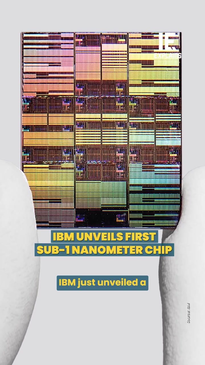
IBM Sub-1 Nanometer Chip
The IBM Sub-1 Nanometer Chip represents a groundbreaking advancement in chip technology, marking the entry into the angstrom era. This tiny chip, measuring just 0.7 nanometers, or 7 angstroms, fits nearly 100 billion transistors within an area roughly the size of a fingernail. This leap in technology promises significant improvements in performance and energy efficiency, with potential applications ranging from generative AI to cloud infrastructure.
Context
The unveiling of the IBM Sub-1 Nanometer Chip signals a transition from the nanometer to the angstrom scale. This shift is crucial as traditional chip scaling faces physical limitations. By moving to 0.7 nanometers, IBM has achieved a density nearly twice that of their previous 2-nanometer chip, introduced in 2021. This new architecture, named nanostack, significantly enhances the chip's performance and efficiency.
Main discussion
The Significance of Sub-1 Nanometer Chips
The development of a sub-1 nanometer chip is a milestone for the semiconductor industry. To understand the scale, consider that a strand of human DNA is 2.5 nanometers wide, making this chip smaller than the width of a DNA strand. This tiny size allows for an unprecedented level of transistor density, packing nearly 100 billion transistors into a small area.
Nanolayers
IBM's nanostack architecture enables the high density of transistors by stacking multiple layers vertically. This innovative approach to chip design allows for more transistors to be incorporated within the same footprint, resulting in a denser and more powerful chip. The vertical stacking also improves performance by reducing the distance electrical signals need to travel, thereby decreasing latency and increasing speed.
Performance and Efficiency
The IBM Sub-1 Nanometer Chip is projected to offer up to 50% more performance or 70% greater energy efficiency than the previous 2-nanometer chips. This leap in capability is particularly significant for applications that demand high computational power and low energy consumption, such as generative AI, cloud infrastructure, and next-generation electronic devices. The enhanced performance and efficiency make this chip a game-changer for various industries, from data centers to consumer electronics.
Applications
The potential applications for this advanced chip are vast. Generative AI, which requires massive computational resources, will benefit significantly from the increased performance. Cloud infrastructure will see improved efficiency, reducing operational costs and environmental impact. Next-generation electronic devices, such as smartphones and wearable technology, will also benefit from the increased performance and energy efficiency, leading to more powerful and reliable devices.
Production Timeline
IBM estimates that production of this groundbreaking chip could commence within the next five years. This timeline reflects the complexity and precision required to manufacture sub-1 nanometer chips. As the industry continues to push the boundaries of what is possible, the transition to sub-1 nanometer technology will require advancements in manufacturing processes and materials.
Practical Tips
Understanding Nanometer and Angstrom Measurements
To grasp the significance of the IBM Sub-1 Nanometer Chip, it is essential to understand the scale of nanometers and angstroms:
- Nanometer: A nanometer is one billionth of a meter (10^-9 meters).
- Angstrom: An angstrom is one ten-billionth of a meter (10^-10 meters), which is ten times smaller than a nanometer.
Comparing Chip Sizes
To put the size into perspective, compare the IBM Sub-1 Nanometer Chip to common objects:
- Human DNA: A strand of human DNA is approximately 2.5 nanometers wide, making the 0.7-nanometer chip smaller than a single strand of DNA.
- Grain of Sand: The chip is smaller than a grain of sand, illustrating the incredibly tiny scale of this technology.
Benefits of Vertical Stacking
The nanostack architecture is a key innovation in this chip. By stacking layers vertically, manufacturers can fit more transistors into a smaller space, increasing density and performance. This approach also improves efficiency by reducing the distance electrical signals need to travel, leading to faster and more reliable computing.
Important takeaways
The Future of Chips
The IBM Sub-1 Nanometer Chip represents a significant advancement in chip technology, marking the transition from nanometer to angstrom scales. This innovation is crucial for the semiconductor industry, which faces physical limitations in traditional chip scaling. The high density and performance improvements make this chip ideal for next-generation applications, from generative AI to cloud infrastructure.
Energy Efficiency
One of the standout features of this chip is its energy efficiency. With up to 70% greater efficiency than previous generations, this chip promises to reduce operational costs and environmental impact, making it a sustainable choice for data centers and other high-performance computing environments.
Industry Implications
The introduction of sub-1 nanometer technology has far-reaching implications for the semiconductor industry. It signals a new era of innovation, pushing the boundaries of what is possible in chip design and manufacturing. This advancement will drive progress in various fields, including AI, cloud computing, and consumer electronics.
Conclusion
The unveiling of IBM's Sub-1 Nanometer Chip represents a significant milestone in semiconductor technology, marking the transition to the angstrom era. This chip, with its unprecedented transistor density and performance improvements, opens new horizons for applications ranging from AI to cloud infrastructure. The nanostack architecture and vertical stacking innovations are game-changers, paving the way for more powerful and efficient electronic devices. As production commences within the next five years, the industry can look forward to a new era of technological advancements driven by this groundbreaking chip.
Watch the Reel
Questions readers ask
What makes the IBM Sub-1 Nanometer Chip a significant breakthrough?
The IBM Sub-1 Nanometer Chip is significant because it measures just 0.7 nanometers, or 7 angstroms, making it the world's first chip to enter the angstrom era. This breakthrough allows for a higher transistor density, with nearly 100 billion transistors fitting into a area about the size of a fingernail, which leads to improved performance and energy efficiency.
How does the size of the IBM Sub-1 Nanometer Chip compare to previous chip technologies?
The IBM Sub-1 Nanometer Chip is considerably smaller than previous chip technologies. It's nearly twice as dense as IBM's prior 2-nanometer chip, demonstrating a major leap in miniaturization and transistor density.
What are the potential applications of the IBM Sub-1 Nanometer Chip?
The potential applications of the IBM Sub-1 Nanometer Chip are vast and include advancements in generative AI, enhancements to cloud infrastructure, and improvements in various high-performance computing tasks. Its increased performance and energy efficiency make it a promising technology for a wide range of industries.
What challenges does the IBM Sub-1 Nanometer Chip overcome in chip technology?
The IBM Sub-1 Nanometer Chip addresses the physical limitations of traditional chip scaling by transitioning to the angstrom era. This shift allows for a higher density of transistors, which is crucial for improving performance and energy efficiency in an era where traditional nanometer scaling is becoming increasingly challenging.
How does the IBM Sub-1 Nanometer Chip impact energy efficiency?
The IBM Sub-1 Nanometer Chip significantly impacts energy efficiency by allowing for a higher transistor density within a smaller area. This increased density enables more efficient processing, reducing the overall energy consumption required for computational tasks. This makes it a promising technology for energy-conscious applications.
What is the significance of the 0.7 nanometer measurement in the IBM Sub-1 Nanometer Chip?
The 0.7 nanometer measurement, or 7 angstroms, in the IBM Sub-1 Nanometer Chip signifies a major milestone in chip technology. It marks the first time a chip has entered the angstrom era, allowing for unprecedented levels of miniaturization and transistor density. This measurement is crucial for achieving significant advancements in performance and energy efficiency.
What is the expected impact of the IBM Sub-1 Nanometer Chip on cloud infrastructure?
The IBM Sub-1 Nanometer Chip is expected to have a significant impact on cloud infrastructure by enhancing the performance and efficiency of cloud-based services. Its higher transistor density and reduced energy consumption can lead to faster processing speeds and lower operational costs, making it a valuable technology for cloud providers and users alike.
Related deep dives
Similar reads based on topic and creator.


Recent articles
Fresh deep dives from the latest Reels we unpacked.




Comments
Be the first to comment.